Overview:
Driving by the needs of future micro/nano-electronic devices with low energy 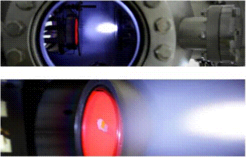 consumption, high storage density and high write-read speed etc., much effort has been spent on the searching for novel materials/structures as substitutes to the traditional semiconductors. In recent decades, functional oxide materials, exhibiting exotic physical properties such as high Tc superconductivity, colossal magnetoresistance, ferro/piezoelectricity and multiple ferroics etc. are expected to be the promising candidates for the next-generation applications such as data storage, energy conversion, or sensing/actuation. Under this circumstance, our research focuses on the oxide-based nanoelectromechanical, electronic and spintronic structures with a control of atomic precision, exploring the emerging phenomena at the surface and interface, domain and phase boundaries of functional systems such as ferroic or multi-ferroic oxide-based structures at their reduced dimensions.
Material Growth with an Atomic Precision.
A precise control of high-quality oxides and oxide-based structures are usually the prerequisite for probing the emerging physical phenomena and their future controls by external stimuli. Here, multiple ways such as pulsed-laser deposition, laser molecular beam epitaxy, chemical vapor deposition, evaporation, sputter, etc. are used to synthesize novel materials and structures. With those growth controls, it is possible to study the crystal structures and physical properties under the epitaxial constraint or various surface/interface states. Examples of the growth of the complex oxide and metal/oxide heterostructure are shown.
Layer number control by Reflection High-Energy
Electron Diffraction(RHEED)
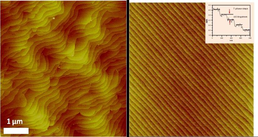
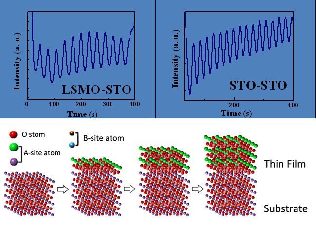
Further more, using reflection high-energy electron diffraction(RHEED), we are able to accurately control the layers of thin films by monitoring the oscillations in real time. High-quality interface can be prepared with the modulation of the termination. such as STO films on STO, or LSMO films on the substrate of STO, which has been shown on the left.
Nanoscale Control of Multiple Ferroic Orders.
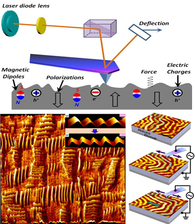
The eventual goal for achieving the possible device application is the control of those order parameters and functionalities (e.g. ferroelectricity, magnetism, flexoelectricity, elastic deformation or multiferroicity etc.) at nanoscale. Scanning probe technique is not only a tool to explore those physical behaviors at nanoscale, but also provides multiple stimuli such as electric field, current, thermal gradient, mechanical force etc., which can be used to manipulate those multiple order parameters in oxide-based systems. As shown in the images below, structural phase boundaries and magnetic domain walls are deterministically controlled by the nanoscale tip-induced mechanical and electrical stimuli respectively.
Emerging Phenomena at Interface, domain walls
or phase boundaries.
“The interface is the device”, as said by Nobel Laureate Herbert Kroemer. Interface, phase boundaries or domain walls in oxide-based functional systems usually exhibit exotic behaviors such as the 2-D electron gas in insulating interfaces or largemagnetoresistance across multiferroic domain walls etc., which are absent in their bulk counterparts. Those nanostructures can be artificiallycreated by using crystal growth conditions or probe techniques. Taking advantage of the micro/nano-fabrications, prototype devices based on those boundaries can be formed, which provides an excellent platform to design possible conceptual applications.